M
ulti
cores
Multi core
MCU
Target
MCUs are F28P65xD, F2827xD, F2838xS and
F2838xD.
Predefined symbols
Predefined symbols such as CPU1, CPU2, CM and _FLASH
are referred in easyDSP source files when multi-core MUC is used.
If target core is CPU2, CPU2 should be predefined. If
target core is CM, CM should be predefined.
These symbols are usually predefined by CCS. But
please check.

Using
debugger
Don't use multi-core booting related functions
(easyDSP_Boot_Sync) easyDSP is providing in case you use debugger.
Debugger will load the memory of each core. please refer to #define
USE_DEBUGGER of main.c in easyDSP source file folder.
easyDSP uses
MCU resource for multi core Ram booting
Some MCU resource is used by easyDSP to implement
CPU2/CM ram booting. Please check below table. You should not use these
resource before CPU2/CM booting (calling of easyDSP_Boot_Sync() function) in
your code. But you can use them after the booting.
| MCU |
F2837xD |
F2838xS
F2838xD |
F28P65xD |
Resource
used by easyDSP
during
ram booting CPU2 and CM |
IPC_FLAG0
IPC_FLAG5
IPC_FLAG31 |
IPC_FLAG0
IPC_FLAG5
IPC_FLAG6
IPC_FLAG30
IPC_FLAG31
CPU1 to CPU2
MSGRAM1
CPU1 to CM MSGRAM1 |
IPC_FLAG0
IPC_FLAG5
CPU1 to CPU2
MSGRAM0 |
Flash booting location of F2838x
and F28P65xD for CPU2 and CM
In the source file of
easyDSP, the flash booting location is fixed :
For F2838xD CPU2 and CM,
it is set to sector 0.
For F28P65xD CPU2, it is set to bank
3.
In case you like to change its location, please modify below part in
easyDSP_Boot_Sync() function in the easyDSP source file.
F2838x
BitField
:
ezDSP_Device_bootCPU2(BOOTMODE_BOOT_TO_FLASH_SECTOR0);
ezDSP_Device_bootCM(BOOTMODE_BOOT_TO_FLASH_SECTOR0);
F2838x DriberLib
:
Device_bootCPU2(BOOTMODE_BOOT_TO_FLASH_SECTOR0);
Device_bootCM(BOOTMODE_BOOT_TO_FLASH_SECTOR0);
F28P65xD BitField :
ezDSP_Device_bootCPU2(BOOTMODE_BOOT_TO_FLASH_BANK3_SECTOR0);
F28P65xD
DriverLib :
Device_bootCPU2(BOOTMODE_BOOT_TO_FLASH_BANK3_SECTOR0);
Restriction of memory use for RAM booting of F2838x and F28P65xD
RAM booting via SCI port for CPU2 and CM of F2838x and
F28P65xD is not supported by TI. easyDSP uses workaround to boot CPU2 and CM
via SCI. First, boot CPU1 via SCI with user program then boot
CPU2/CM with small agent program (not user program) via 'IPC message copy
to RAM' boot mode. Then this agent program downloads user program to CPU2 and
CM via SCI. With this, there is some restriction of memory usage to CPU2 and
CM for this agent operation. Please check below table and reflect this to
command file accordingly.
| |
Restriction of memory usage in user program
when ram booting of F2838x |
Restriction of memory usage in user program
when ram booting of F28P65xD |
|
CPU1
user program |
no
restriction |
no
restriction |
|
CPU2
user program |
part of
M1 RAM (0x400 - 0x7F7) can't be used as initialized
section |
part of
M1 RAM (0x400 - 0x5FF) can't be used as initialized section |
|
CM
user program |
part of
S0 RAM (0x2000.0800 - 0x2000.0FFF) can't be used as initialized
section |
|
Change in CPU2 RAM booting of F2837xD and F2838xD from easyDSP
source file version 11
Before easyDSP source file version 11, for CPU2 ram
booting of F2837xD and 2838xD, all the GSRAM (Global Shared RAM) are allocated
to CPU2 during CPU2 ram booting and then allocated to CPU1 after ram
booting in the easyDSP_SCIBootCPU2() function of easyDSP source file.
So,
ram booting related code of CPU1 (.text section of easyDSP_SCIBootCPU2()
function) should be located to LSRAM (Local Shared RAM). And if required from
CPU2 user program, CPU1 should allocate GSRAM to CPU2 after CPU2 ram booting.
This way requires lots of restriction and caution and not any longer
recommended.
In the source file version 11, GSRAM is
allocated to neither CPU1 nor CPU2 in the easyDSP_SCIBootCPU2()
function.
Instead, in the CPU1 program main.c, the required GSRAM is
allocated to CPU2 before calling easyDSP_SCIBootCPU2().
With this, no more
restriction and caution
needed.
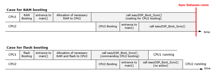
Booting sequence and syncronization of F2837xD and F28P65xD
The flash booting is executed in a sequence
of CPU1 and then CPU2 without any synchronization between.
The RAM booting is executed in same
sequence with synchronization (i.e. the end of easyDSP_Boot_Sync() is
synchronized).
Note that necessary memory should be
allocated to CPU2 before CPU1 is calling easyDSP_Boot_Sync().

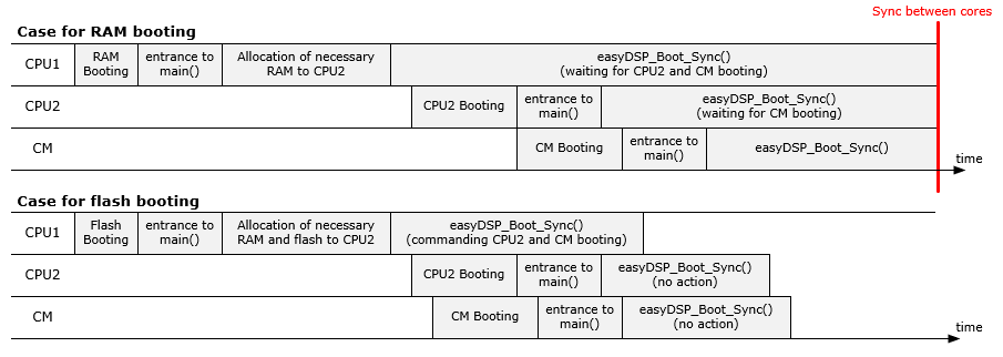
Booting sequence and syncronization of F2838x
The flash booting is executed in a sequence
of CPU1, CPU2 and CM without any synchronization between.
The RAM booting is executed in same sequence with
synchronization between (i.e. the end of easyDSP_Boot_Sync() is
synchronized).
Note that necessary memory should be
allocated to CPU2 and CM before CPU1 is calling easyDSP_Boot_Sync().

F2838x CPU2 and CM clock
When CPU1 boots CPU2 and
CM,
CPU1 set their clock frequency to 200MHz and 125MHz respectively. If you like to change them, you
should modify the related source file by yourself.
When out file has been changed
The output file (*.out) is changed whenever the
user program is compiled. When you download the new output file by either RAM
booting or flash programming in the easyDSP project connected to CPU1,
the easyDSP project connected to another cores should be updated by new output
file too.
In case easyDSP for multi cores are all
connected to the same PC, this process is done automatically, meaning easyDSP
project for CPU1 asks easyDSP project for CPU2 to load new output file.
In case they are open in different PC, you have to load new
output file for another cores manually, by clicking 'MCU > Reload *.out'
menu.


